I met some great people today, and I also got a wonderful device for my ongoing experiments as a gift: The UT50 Scintillation probe, manufactured by SC ICPM SA Romania. It features a huge NaI(TL) crystal, with a diameter of 5.5cm and 5.5cm length. The photomultiplier is a British EMI9656KB and the entire device is encapsulated in an aluminum modular cylinder of no more than 24cm total length and 1270g weight. Considerably more compact than my previous NaI Scintillation probe, and with a bigger crystal. But the device only contains the crystal, the photomultiplier, and the voltage divider, exposing a BNC connector, so I will need to build the high voltage supply, the signal preamplifier and the counter, for a complete gamma spectrometer. I could either design it to use a computer, or build a standalone micro-controller based unit. My final choice was to use a bluetooth UART module, and export all data to an Android phone, that shows the Gamma Spectrum and all the relevant details.
Pictures
The following pictures show the probe assembly:
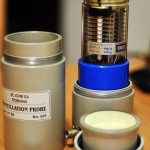
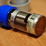
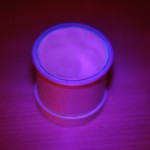
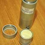
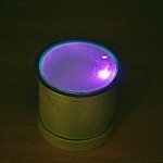
The violet-colored images show crystal fluorescence under UV light, from a torch (third picture) and from a UV laser beam (last picture).
The Photomultiplier EMI9656
The voltage divider is consistent with EMI’s “Photomultiplier tubes & Windowsless Electron Multipliers” that shows a separate circuit topology for a “Photomultiplier standard Dynode Chain (eg.9656 used in scintillation counting)”, see Fig.5a from page 12 of the document.

For the EMI 9656KB, the base pins are as follows:

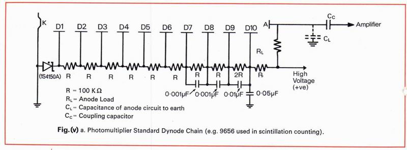
The IS4150 (Texas) is a 10W 150V Zenner Diode. The same document comes with additional useful information. I will use that when designing the high voltage supply, but also the signal amplifier.
August 11, 2013: The high voltage supply
The EMI specs show the following tube characteristics:
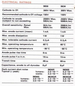
The specs also indicate that for the 9656 photomultiplier the typical anode -cathode voltage is 1200V with a maximum of 1650V (page 30).
But my plan is to be able to connect various scintillation probes to the counter I’m building, so the High voltage supply should be adjustable in software. For the UT50 I will use 1200V, but the supply should be able to go as high as 2000V. For this I’ve built a ferrite core transformer that will be driven by PWM signal generated by the microcontroller. Changing the duty cycle will allow a precise control over the output voltage. The ferrite transformer uses an A22 core (2100 factor), 16 turns in the primary (0.2mm CuEm wire) and 600 turns in the secondary (0.08mm wire):
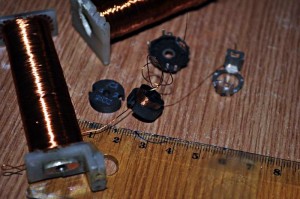
This transformer could easily output more than 1000V by itself, but to lower the stress on the wire insulation, I will add a 3 stage voltage multiplier, to rectify the output.
August 26, 2013: The circuit and the PCB
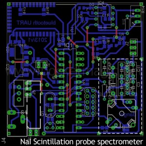
I’ve finally been able to finish the circuit and the PCB design. Not easy, but finally I have everything in place:
– the power supply: 3-5V with inverter and regulator both for battery and power adapter use;
– the digital temperature sensor: for compensating the temperature drift;
– the Bluetooth module for interfacing with the Android phone;
– the regulated high voltage module: PWM driver, ferrite transformer (see above), 4 stage voltage multiplier with voltage feedback on level 1 for regularization, output high voltage capacitor as filter;
– PMT preamplifier with 2 bipolar transistors
– sample and hold circuit for converting the PMT pulses to digital via ADC, using the LM358 op amp.
– small size: using SMD components, the entire board is only 6 x 6 cm big!
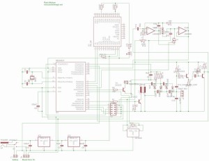
The sample and hold circuit
This spectrometer registers the pulses produced by the photomultiplier, as a result of radiation passing through the scintillation crystal. More details here. Besides counting the number of pulses and measuring the time, like we do with Geiger Counters, we are interested in knowing the amplitude of each pulse, and use the data to compute the Gamma spectrum. This is possible, because the pulse amplitude is proportional to the incident radiation energy level.
Measuring the pulse amplitude implies using the microcontroller’s ADC ports for converting an analogue value to a digital one that is further used in software processing. The timing becomes an issue: the PMT pulses are very short lived, somewhere close to 1 micro second, while converting the pulse amplitude using the ADC mechanisms requires a lot more, up to 20 micro seconds: so by the time we are done with the pulse amplitude measurement the pulse is no more, being replaced with the subsequent pulses. Obviously, this would not work – the solution is to use a sample and hold mechanism, to grab the pulse voltage value (amplitude) and keep it in a buffer right until the conversion is complete.
To do this, we can use a dual operational amplifier, such as the LM358, TL072, etc, and a capacitor with very low leakage:

A typical sample and hold circuit stores electric charge in a capacitor and contains at least one fast FET switch and at least one operational amplifier.[1] To sample the input signal the switch connects the capacitor to the output of a buffer amplifier. The buffer amplifier charges or discharges the capacitor so that the voltage across the capacitor is practically equal, or proportional to, input voltage. In hold mode the switch disconnects the capacitor from the buffer. The capacitor is invariably discharged by its own leakage currents and useful load currents, which makes the circuit inherently volatile, but the loss of voltage (voltage drop) within a specified hold time remains within an acceptable error margin. More here.
Here is the circuit diagram:
The Bluetooth module
Using a bluetooth module , this spectrometer will be able to communicate with an Android phone for exporting the data and to take advantage of the nice color display, touch screen capabilities and impressive processing power given by the smartphone. A lot better than using a tiny screen hooked directly to the AVR microcontroller.
September 01, 2013: Making the board
Using toner transfer, I created a few PCBs, using the design above:
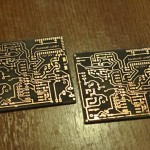
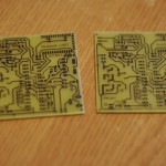
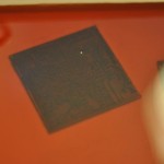
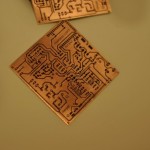
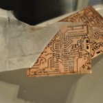
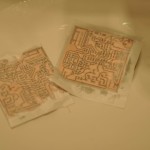
Then my favorite part, soldering the components, mostly SMDs so a lot of attention got involved in the process.
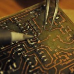
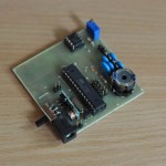
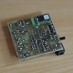
September 02, 2013: The code and a first test
Having the board ready, couldn’t wait to test it. But first, I had to write the code for the microcontroller: the inverter module with the PWM generator and the voltage feedback for regularization, the UART code for communicating with the Bluetooth Module, the DS1820 Temperature sensor code, and some basic logic for debugging the important parameters over the bluetooth connection. It all worked at the first try, and I was able to reuse most of the code from my previous similar projects, uRadMonitor, the portable Digital Dosimeter, or the Kickstarter project. Having the bluetooth link working , all vital data could be visualized using a serial connection in Putty:
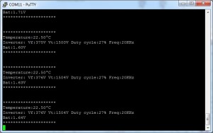
The Pic shows the output high voltage being set to a 1500V threshold. For my probe I’ll need to set it anywhere between 1200V and 1650V as presented above.
The voltage feedback is taken at the first rectification stage, out of the total 4 added in the multiplier block. It would have been better to take the measurements directly on the output, but this would have been more complicated because of the high voltage. Even so, the voltage stays in a given tolerance interval, and will be improved by adding a higher capacitance for the final filter (C12 see diagram).
The Inverter frequency has been set to 20KHz, but this can be easily changed in the software:
/************************************************************************/
/* Configuration                                                        */
/************************************************************************/
#define INVERTER_DEFAULT_DUTY	270// change it to provide as close to target as possible, before regularization
#define INVERTER_DUTY_MIN		5// inverter duty cycle will not go below 0.5%
#define INVERTER_DUTY_MAX		1000// inverter duty cycle will not go above 40%
#define INVERTER_FREQUENCY		20000UL// inverter frequency in Hertz
#define MULTIPLIER_STAGES		4// use 1 if no multiplier
#define TARGET_VOLTAGE			1500// inverter output voltage
#define INVERTER_THRESHOLD		(TARGET_VOLTAGE / MULTIPLIER_STAGES)
#define INVERTER_TOLERANCE		5// tolerance for adjusting the duty cycle to control the voltage
September 03, 2013: Changing the UT50 resistive divider
Hooking the probe to the HV supply resulted in failure: the probe would refuse to return any pulses. At this point there can be only two possible causes, that I need to rule out: either the resistive divider is malfunctioning, or the PMT tube is dead.
The first one is easy and I wanted to do it anyway: changing the old resistors and caps to newer, better quality components:
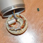
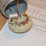
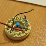
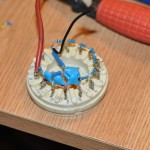
However this didn’t help. As I don’t have another EMI9656KB tube to replace the current one, I will have to connect a different tube, such as any of my other photomultipliers and identify the problem that way.
To be continued.

“the probe would refuse to return any pulses” – Your dynode string really uses 100k resistors? Your HV Source must then be able to supply more then 1mA at 1000V. I’m sure you checked, but are you sure that your HV didn’t drop to a few 100V after the doubler stages?
You are right Katze, there is a considerable voltage drop, didn’t have time to post updates with all the uRADMonitor work, but will soon.
In the pics above I merely changed the original resistors with newer ones, as you see in the EMI doc included at the beginning of the post those were the recommended values.
Quickly looking over my notes from September 03 (yes, I still use paper for that..), I see I recorded the following drop values on my inverter’s output:
1500V->250V on 1MO load (!!!)
1500V->800V on 4.7MO
1500V->1100V on 10MO
So I’ll have the resistors changed and report back when I get some time. Hopefully the current will be enough for the PMT to work as expected.
Bicron suggests 100k resistors, too, here: http://www.detectors.saint-gobain.com/uploadedFiles/SGdetectors/Documents/Electronics/Voltage-Divider-Design-Considerations.pdf – the current through the voltage divider then is very large compared to the tube current. For best results this will be desirable, but you will still get good results with much larger resistors (e.g. a chain of 1MOhm resistors), which is much better to handle for a mobile battery-powered device.
Time is the only problem. Soon, hopefully, will post some updates.
Salut Radule.
Omule am intrat in posesia unei placi construite de cineva prin 2006, care a fost un proiect pentru a masura curenti de absortie-resobtie-conductie pentru transformatoarele de inalta tensiune.
Pe baza placii am refacut o mare parte din shema in Eagle. Partea de masura a curentilor foarte mici care trec prin izolatia din transformator dupa ce aplici 500 sau 1000 sau 2000V, este masurata cu un circuit pe baza de LOG104 (azi exista LOG114).
Treaba foarte interesanta este ca toata bucata de masura a curentilor este cu masa flotanta si izolata capacitiv cu ISO124 de placa de achizitie.
Alimentarea acestei bucati se face cu convertoare DC-DC izolate, alimentate la 5V si care scot +-12 si comun.
Ma ajuti sa dau de cap acestei placi?