Building a Geiger clicker is somewhat easy assuming the maker can procure two essential components: a geiger tube and the high voltage supply. As most detectors are portable and made to operate on batteries, the high voltage supply is usually conceived as a high frequency inverter, that boosts the DC low input voltage up to the high voltage required to operate the Geiger Muller tube.
In my circuits I usually go with Russian Geiger tubes, and most of them use 400V. So this is why I’ve designed the circuit presented here, as a high efficiency 3V to 400V inverter, with extremely low ripple.
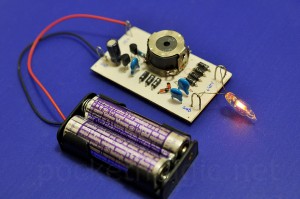
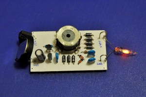
The circuit is based on a modified Armstrong oscillator, a small ferrite transformer with a feedback coil for the oscillator, a blocking transistor commanded by an array of zener diodes. The diodes dictate the output voltage and are part of the regulating block, responsible for outputting precisely the selected voltage. When building Geiger counters, the voltage control is important, in order to protect the tube which can be affected negatively by uncontrolled voltage. This topology also ensure a high efficiency, while it only requires a couple of simple components, unlike the more complicated inverter circuit presented a while ago.
The circuit details
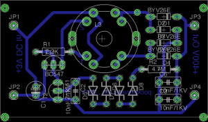

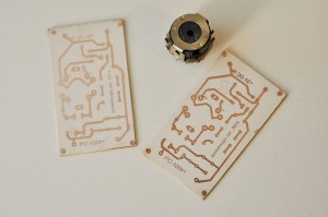
Download the Eagle files and the PCB pdf, here: geiger_high_voltage_3V_400V_supply
The ferrite core transformer
This is also easy to make, although some people are really scared about making their own transformers. You’ll need 16 turns for primary, 16 for the feedback coil, and 650 turns for the secondary. We are not using any voltage multipliers in this circuit, so the high ratio is needed to be able to make the big jump from 3V to 400V. The wire diameter is 0.2mm for the primary and feedback and 0.08mm (very thin!) for the secondary. Careful to add proper insulation, as 400V is enough for internal arcing that could ruin hours of work. Also note that the transformer will work in flyback mode, so a tiny piece of paper must be added between the two ferrite pieces for a minimum of distance.
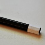
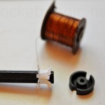

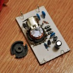
I improvised a coil former using paper, on a hex key, matching the internal diameter of the ferrite core. Cutting some edges I got a nice support, where the wire will not fall down while winding. I scrap the wires from old relays, but I advise you to use new wire with a good insulation if possible. What I had worked perfectly anyway.
The core I’ve used is an old 18mm diameter, A22 type core, with AL=2800 .
Critical components
The T1 transistor (MPSA18) is absolutely vital for this circuit. I usually design devices allowing considerable freedom in changing some of the parts, but for this design, you absolutely must use the MPSA18. Here’s an output comparison list, with various transistors used instead of T1, on an input of 3V DC:
T1: MPSA18 – 3V in gives 384V, maximum selected by the zener diodes, clearly the transformer puts out a few tens of volts more
T1: 2n5551 – 3V gives only 152V, the regulator section doesn’t even fire
T1: 2n4401 – 3V gives 328V, nice, but not enough
T1: 2n2222 – 3V gives 284V, again too low
T1: BC548 – 3V gives 220V, only
As you can see the MPSA18 makes a huge difference. With the MPSA18, the circuit will oscillate even at 1.5V, outputting 236V!
The Zener diodes connected in series will control the output voltage. For my boards I used 3x 120V Zeners + 2x16V and got 384V output , considering there’s a little voltage drop across them. YOu can use any configuration needed. You can also replace the rectifier diodes with a multiplier block in case you need higher voltages, or simply increase the input voltage. The way this works is that when the output voltage is greater then the cumulative zener threshold, the diodes will open the T2 transistor that will block T1, stopping the oscillation, so the voltage will drop. This feedback mechanism, coupled with the output filter capacitors, C3 and C6 will assure we have a constant output voltage, regulated to the value allowed by the Zener diodes.
The R1 resistor, controls the output max current, but also the consumed current. The lower the value, the more current will flow through the T1 and the transformer. Higher current will result in heating, so change this carefully and only if needed.
Selecting the voltage
As presented above, changing the Zener diodes will impact the output voltage. You can use 4x 100V zeners connected in series for 400V output (D5, D6, D7, D8 in the diagram). For my circuit I used 3x120V + 2x16V and got an output of 384V, just perfect to operate Russian Geiger tubes.
Some measurements
The following pictures show the output voltage and the input current:
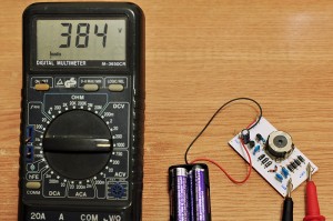
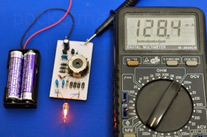
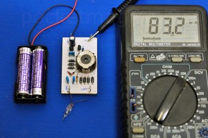
384V output, 128mA with a neon bulb load (high consumer), 83mA with no load all at only 3V input. These values were collected with R2 set at 4.7K . For the current value presented in the schematics (6.8K), the consumption is even lower, it gets down to 50mA. This can be decreased even further if needed, by changing R2 up to 10K. There’s a limit though, as setting R2 too high , will stop the oscillation and the inverter won’t work.
Oscillographs
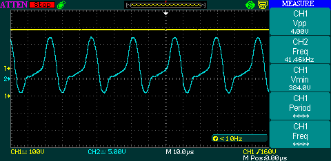
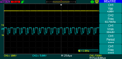
The following are screenshots from my o-scope, CH1 (yellow) shows the output voltage and the nice constant value, while the CH2 (cyan) has been connected to T1’s collector in the first picture (showing the driving frequency), and to T2’s collected in the second picture (showing the regulation frequency).
Update
The MSPA18 is running close to its limits and this can shorten its life. We can replace it with the more robust T1:C1008, while also changing the R1 to 2.7K
With this modification, the circuit draws 70mA in idle mode and 130mA with the neon bulb connected.
Demo video
A quick test circuit, probably the simplest Geiger clicker circuit, with just a tube, a limiting resistor and a Piezo speaker.
Careful, most of the energy stored in the capacitor will be dumped in the tube, and that will come as a high current burning the quenching gas. This circuit was meant just for a few seconds demo, do not build a counter this way.

The limited voltage with different transistors is almost certainly due to variations in breakdown voltage, not gain. The MPSA18 is rated at 45V the BC548 is only 30V. Trying a BC546 rated at 60V compared to a BC548 would be a more useful comparison especially if you selected examples with similar gain. I know your ‘scope is only showing about 20V at the transistor collector, but the base is minus 5V. As I don’t know the exact setup, scope and probes used, it is possible it is not showing the true peak voltage, and the transistor is breaking down. The circuit must be relying on flyback as the transformer ratio is just 40.625 to 1 so maximum transformer action peak voltage is 122V. The transistor is being over stressed in this design. 50mA off load is very high for this type of circuit, never mind 80mA. My CCFL based circuit ( Google g8rpi ccfl ) only consumes 20mA at 3.5V input for 900V output and 90uA load. I’m sure a lot of work went into this and am sorry to be negative, but this has all the signs of a circuit that was made to work rather than designed to work. Why is C2 rated at 1kV? The most positive it will see is about 720mV (VBE) and negative is about 10V (VEBO breakdown).
Robert G8RPI.
Hi Robert, thanks for the knowledgeable answer, much appreciated. We probably need the transistor replaced as it’s pushed to its limits. It was one of the few options available in my toolbox. But as explained in the article (and also visible on the schematics), the current can be reduced by increasing the value of R1 to an extent where it will not impact the output voltage. The transformer is working in flyback mode. I used a little piece of paper placed between the two sides of the ferrite core as shown in the photos. The Zeners do an excellent work at regulating the output voltage.
I’ve looked over your “G8RPI+CCFL+BASED+HV+SUPPLY.pdf” diagram, correct me if it’s not the right document. I see you’re using a Royer oscillator, powered via a LM317 and there’s a voltage doubler on the output.
If you’re “regulating” the supply via that LM317, you’ll never know what your output voltage is, unless you use a multimeter to measure it and that causes a voltage drop, complicating the operation for the not so experienced. Then we’ll also have the problem of stability as the voltage will drift from its initial value because of heating components. Probably all SMPS use a feedback mechanism connected to the output voltage and there is a good reason for that. I believe you could easily adapt it to implement some kind of feedback mechanism connected on the output.
Regarding the voltage doubler, I could have used a voltage doubler, tripler or even higher multiplying stages in my design too. Than I could have reduced stress on the transistor and lower the input voltage (down to 1.5V no problem) and the current to just a few mAmps. That might be ok for some applications, but it also induces a lot of ripple on the output. Personally, I wanted to avoid a multiplier where possible.
Hi Radu,
My comments were intended to be constructive, not just critical. The claims of “perfect” and “high efficiency” got me to look more closely at your design to see what I could learn. You have found the correct circuit fir my CCFL based design.
While you are correct in saying that it does not have an external feedback loop, this is because it does not need one. This is proven by the voltage change at a nominal 1500V output for a 100:1 change in load (1.5ua 1G ohm to 150uA 10M ohm) is only 28V or 1.87%. I can’t find a figure for output regulation on your design, but a typical small 120V zener, BZX55C120, has a voltage range of 114-127V a range of 13V, more than 10%, you need at least 3 so the zener tolerance alone is 17%.
My design does not need external feedback because the transformer is operating in its linear region, and the circuit impedances are low compared to the load current. Your comment “Most SMPS use a feedback mechanism connected to the output voltage” is not the whole truth. Most multiple output SMPS such as those used in PC’s only regulate the main output, the others track. The main output regulation loop mainly compensates voltage changes at the transformer primary. Many commercial HV DC-DC converters (such as EMCO) do not use a feedback loop, the output voltage tracks the input voltage in the same way as the my design. I used a balanced voltage doubler as it is the most effective circuit for the desired characteristics and presents a balanced load to the transformer, including stray capacitance which becomes very significant at these voltages and frequencies (49kHz). The ripple of my design is 5mV (0.0003%) at full load. Your feedback is very inefficient, drawing at least 5uA (nearly 2W) from the output. From your ‘scope screen shot your ripple is 4V Pk-Pk or 1%. Some of this may by pick-p by the ‘scope probe. It takes very careful setup to avoid this especially with flyback (and square wave driven) circuits which by design have very fast voltage and current changes. This is another reason why I chose a linear, sinewave design. Component heating in my inverter circuit will not significantly affect the output voltage. The critical component is the LM317T which is rated at about 0.0061% per degC or 90mV/ degC at 1500V output. Your zeners are about 0.09% of 120V x 3 = 324mV/degC (no statistical allowance here as they will all drift the same way, unlike the initial voltage tolerance). I’m sorry what you think about me (I won’t repeat it even disguised) but I can’t offer many tips to improve this circuit as its exact design criteria are not clear. My comment on the design being poor highlighted the component choices, but as far as I can tell this circuit is the result of experimentation, not design (I’m being nice here). This is borne out but your belief that the limited output voltage with some transistors was due to their current gain, not breakdown voltage, despite the fact that you could change the base transistor without lowering the voltage. I can’t even guess what transformer design decisions you made as you do not specify (or even know?) the core part number, material or size. As you had to improvise an air gap I assume it was not specifically chosen, but just available. It’s fine to build this for your own use and I think you have done a good job, but I don’t think it’s OK to present it on a website as a “good” design for people who know less than you to copy. This is not an easy task, I’ve been building HV supplies of various types for over 30 years and have had plenty of failures along the way. The CCFL design, while it looks simple is the result of many hours research and design. As a result I’ve built many of these and they have all worked, even using slightly different inverters, without tweaking component values from unit to unit.
Thanks Robert, I’ve added the ferrite core details under “The ferrite core transformer”. Despite the appearances, the truth is I appreciate your knowledge and also the time you put into looking over this, and coming with pertinent suggestions to make it better. It’s just the social part of the game that doesn’t always work ok for me. So regarding what I think about you, be assured everything is fine.